A design can pass its testbench and still be a poor fit for the job: too slow to keep up, too large for the device, or awkward to connect to the next block. My view is that the hardest FPGA decisions often happen before the first line of RTL.
Start with the rate, not the entity declaration
The first useful design document can be a few lines long: input rate, output rate, maximum acceptable latency, clock domains, and what happens when the receiver cannot keep up. Those lines tell me more about the circuit than the eventual length of its VHDL.
Consider a block that calculates two products. If both are needed every clock, two multiplier paths may be a sensible starting point. If a new pair arrives only every fourth clock, a shared multiplier may be enough. The function is the same. The schedule is different.
That is why I put architecture ahead of code volume. Two engineers can write correct RTL for the same calculation and produce very different circuits. Neither design is automatically better; the requirements decide.
A pipeline changes the contract
For y = a × b + c, the multiplication and addition can sit between one pair of registers, or a register can separate them. That boundary changes how much work each clock cycle has to carry.
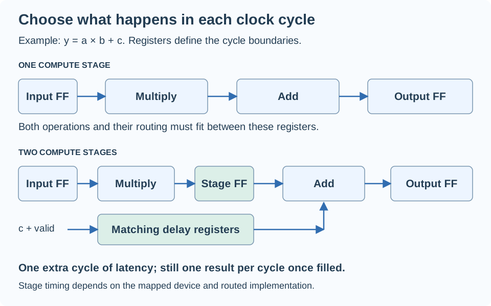
The important detail is the lower path. Registering the product while leaving c untouched can make the adder combine values from different input transactions. A timing improvement that changes the answer is a bug.
I therefore count latency alongside the datapath: data, valid, identifiers, and control. If the interface allows another cycle, pipelining is an option. If the block is in a feedback loop with a strict response deadline, the same change may require a different algorithm or schedule.
There is no promise that one more register will solve timing. A stage can remain overloaded, or routing can dominate. I use the mapped and routed reports to check the choice. AMD’s pipelining guidance discusses distributing long datapaths across cycles; the practical tradeoff is covered further in Throughput vs Latency.
Sharing hardware means owning the schedule
Saving a multiplier sounds straightforward until the surrounding logic is drawn. A shared operator needs operand selection, a schedule, somewhere to keep intermediate results, and a way to associate each result with its destination.
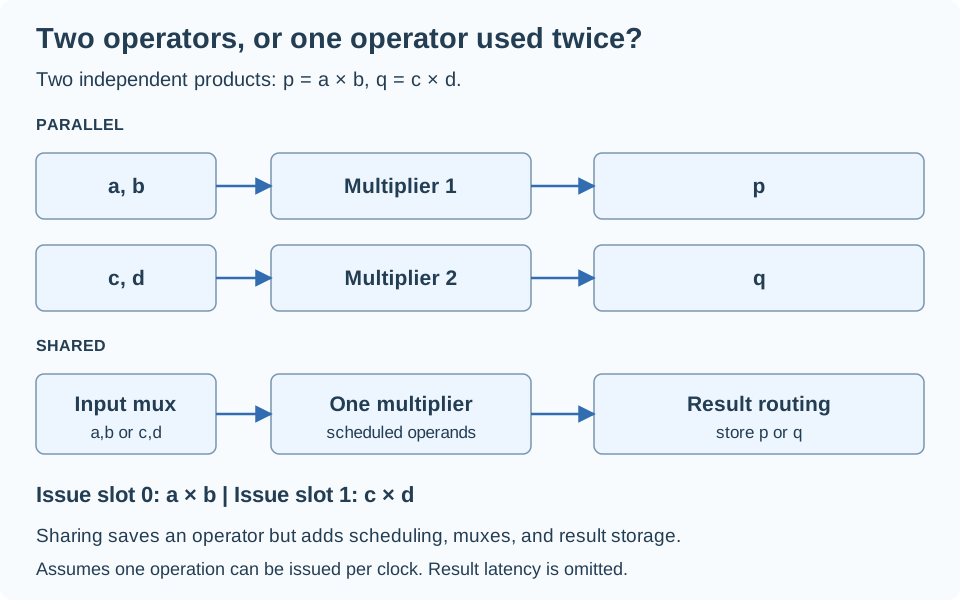
If a multiplier can accept one operation per cycle, two products issued through it occupy two issue slots. A pipeline inside that multiplier affects when the results emerge; it does not create a second input slot. For pairs arriving every cycle, one shared operator at the same clock rate cannot sustain the demand.
I also look at operand widths, signedness, memory ports, and supported DSP or block RAM modes before writing the datapath. A buffer that needs two simultaneous reads has a different architecture from one that needs one read, even when both hold the same number of samples.
Power needs its own check. Sharing can reduce active hardware, but muxes, switching activity, clock rate, and extra registers affect the result. More pipelining can reduce glitches while adding clocked load. A smaller resource count is useful information, not a power measurement.
A clock crossing needs a transfer rule
“Add two synchronizer registers” is a reasonable starting point for some single-bit level signals. It is not a complete plan for moving a data word or a stream between unrelated clocks.
Before choosing the circuit, I ask what must cross: a slowly changing configuration value, an event, or a continuous sequence of samples. Must every item arrive? Can the source wait? What should happen if the destination stops?
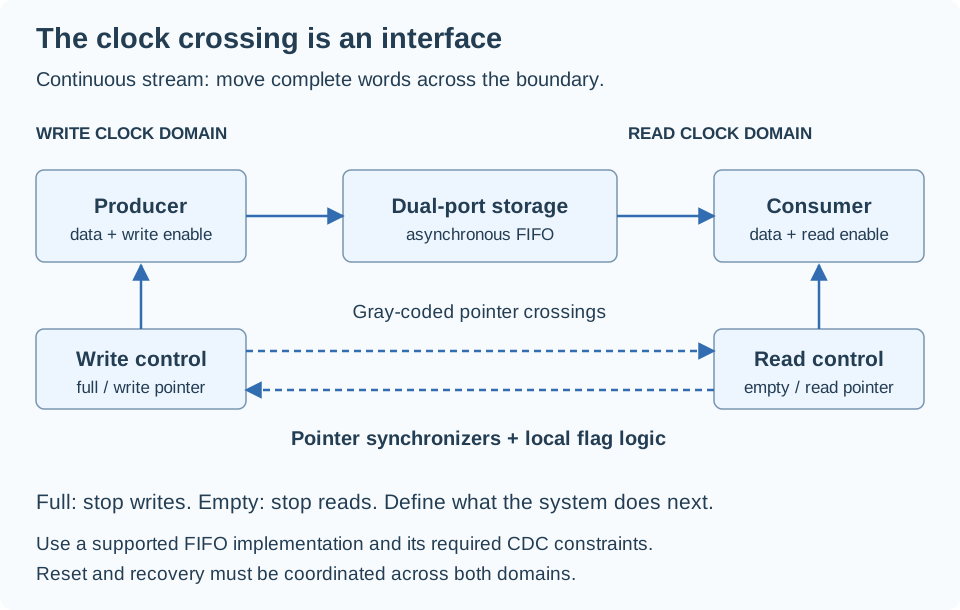
For occasional configuration updates, a supported handshake can hold a word stable until the destination accepts it. For a stream, an asynchronous FIFO provides storage and separate read and write interfaces. Independent synchronizers on every data bit do not preserve a coherent word.
A FIFO also does not fix a permanent rate mismatch. If the producer is faster on average, it eventually fills. The architecture must allow backpressure, deliberate dropping, or a different rate arrangement. I cover coherent transfers in the CDC article, including links to the vendor guidance behind these choices.
Draw the checks while drawing the blocks
I want to know how I will detect a lost sample before I build the sample path. A scoreboard can compare accepted inputs with completed outputs. Assertions can catch a write attempted while a FIFO is full. Random stalls can expose an interface that works only when both ends are always ready.
These checks follow the architecture. A pipeline needs transaction alignment checks. A shared operator needs schedule and result-ownership checks. A clock crossing needs structural CDC review as well as tests of its transfer protocol.
RTL simulation can show that the modeled behavior matches the tests. It cannot establish that the routed circuit meets setup and hold requirements, model analog metastability reliably, or prove that board interfaces will behave as expected. Timing analysis, constraints review, CDC checks, and staged hardware bring-up each answer a different question.
Observability belongs in the design too. A sample counter, an overflow flag, or a deliberate debug tap can make a hardware failure easier to isolate. I would rather decide where those belong than add them after the only visible symptom is a blank display.
Reusable IP starts with a clear boundary
A VHDL file that compiles in a second project is a start. Useful IP also needs an interface that another engineer can integrate without guessing.
I document when a transfer occurs, whether the receiver can stall, how reset affects pending work, and how latency changes with configuration. A generic for data width needs legal ranges and tests at the supported boundaries. “Configurable” should not mean that only the default setting has been checked.
This is where architecture and documentation meet. If the behavior is hard to explain at the interface, it will usually be hard to verify and reuse too.
Architecture, verification, or timing closure?
If I must choose where to start, I choose architecture. It sets the cycle budgets, data movement, resource sharing, and interface rules that the rest of the work must satisfy.
But I would not sign off a design on that answer alone. Verification checks whether the design does the right thing. Timing closure checks whether the implemented circuit can do it at the required clock relationships. Either can reveal that an architectural choice needs to change.
Before opening the RTL editor, my questions are simple: how often does data arrive, how long may it take, where can it wait, and how will I know the result is right? A block diagram that answers those questions earns its place beside the code.
Which of those decisions has cost you the most time to change after integration?